The development of smart devices has followed one unchanging pattern, which requires developers to create functions that occupy smaller areas. Modern electronic devices today encompass both smartphones and smartwatches that, combined with medical implants and Internet of Things sensors, allow manufacturers to create compact products that can deliver advanced technology. This is a big challenge to engineers as they have to devise means of developing complex electronic systems that can be fitted into small spaces and still have the full capacity to operate.
Space-saving rigid-flex PCB circuits have introduced a revolutionary technology to the field. Rigid-flex PCBs combine rigid and flexible circuit technology through their unified design, which enables three-dimensional circuit development while decreasing the need for large wiring components and connectors. The outcome produces lightweight electronic systems that consume minimal space while delivering maximum operational efficiency that suits smart device applications.
The article will examine how space-saving rigid-flex PCB circuits operate while discussing their design principles and manufacturing process, along with their benefits, including essential rigid-flex PCB design tips for optimising performance and space efficiency.
Understanding Rigid-Flex PCB Technology
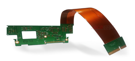
A rigid-flex PCB stands as a specialised circuit board that unites its two distinct components through its two active shapes. Rigid-flex technology establishes an uninterrupted electrical connection that extends through both its solid and flexible components of the design.
Structure Overview
- Rigid sections: Used for mounting components such as ICs, processors, and connectors
- Flexible sections: Used for bending, folding, and interconnecting rigid areas
- Copper traces: Provide electrical connectivity across both regions
- Polyimide substrate: Ensures flexibility and thermal stability
The system provides engineers with a tool that enables them to craft electronic solutions that can adjust their form according to device requirements.
Why Space Optimisation Matters in Smart Devices

Modern smart devices show both declining size and increasing computational power. This creates several design constraints:
- Limited internal space
- Need for multiple sensors and modules
- Requirement for lightweight structures
- Demand for sleek and ergonomic designs
Traditional PCB assemblies often struggle with these constraints due to:
- Bulky wiring harnesses
- Multiple board interconnections
- Mechanical connectors occupy space
- Fixed rigid layouts
Rigid-flex PCBs solve these problems by eliminating unnecessary components and integrating everything into a compact architecture.
Space-Saving Mechanism of Rigid-Flex PCBs
The technology of rigid-flex creates its primary benefit through its capacity to decrease space requirements for both complete systems and their individual components.
Elimination of Connectors
The system achieves its biggest space efficiency through the elimination of both connectors and their associated cables. Traditional systems require connectors to consume substantial PCB space while needing extra mechanical support. Rigid-flex designs replace these with direct circuit continuity.
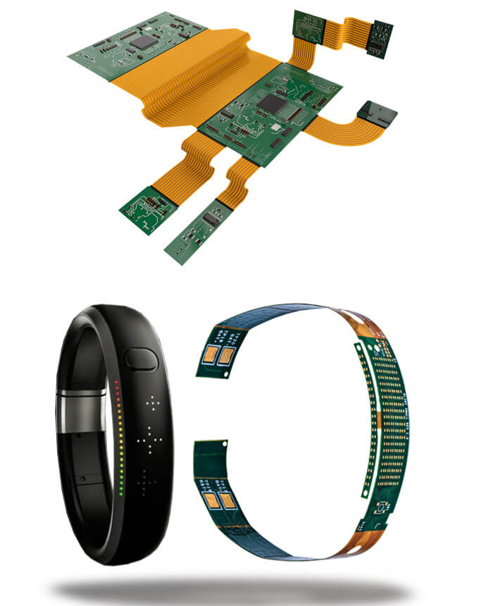
Three-Dimensional Design Capability
Rigid-flex PCBs allow circuits to be folded or bent into 3D shapes. This enables designers to:
- Stack components vertically
- Wrap circuits around device interiors
- Fit electronics into curved housings
Reduced Board Count
A single rigid-flex board handles all functions of multiple PCBs, resulting in reduced space requirements.
Design Principles for Space-Saving Rigid-Flex PCBs
The design process needs to achieve optimal space efficiency while delivering dependable performance throughout smart device operations, which use rigid-flex PCB circuits. Engineers create designs that need small space requirements and strong durability through their work, which connects electrical needs to mechanical design standards.
Layer Optimization
The main approach to achieve this goal involves researchers who need to decrease the layer count without damaging the necessary electrical functionality. The board size decreases through layer count reduction, which improves board flexibility for use in small spaces. Designers need to maintain both power distribution and signal integrity throughout their work.
Strategic Placement of Rigid and Flexible Zones
High-density components, which include integrated circuits and connectors, need to be mounted on rigid sections because those areas provide necessary structural stability. Flexible zones exist to enable bending movements that connect different rigid sections. Proper placement ensures efficient use of space and prevents mechanical stress on sensitive components.
Bend Radius Control
Maintaining an appropriate bend radius is essential for avoiding copper trace damage and material fatigue. The standard practice maintains the bend radius size at 6 to 10 times the board thickness, which guarantees durability during multiple bending cycles.
Trace Routing Efficiency
Trace routing that operates at high efficiency brings benefits for space use and system performance. Designers create trace paths through their selection of smooth curved paths, which they combine with trace length reduction techniques because sharp corners create signal loss problems and need additional space.
Manufacturing Process of Space-Saving Rigid-Flex PCBs
The manufacturing process becomes more difficult to manage because the production of printed circuit boards needs different materials to be integrated into their final product.
Material Selection
| Component | Material | Purpose |
|---|---|---|
| Rigid Layer | FR4 | Structural support |
| Flexible Layer | Polyimide | Bending capability |
| Conductive Layer | Copper | Electrical signals |
| Adhesive | Epoxy/Acrylic | Layer bonding |
Lamination Process
The lamination process serves as an essential procedure for rigid-flex PCB production, which combines rigid and flexible components into a unified system. This procedure requires precise temperature and pressure management to create strong bonds between FR4 and polyimide materials. The correct execution of lamination processes establishes mechanical strength while stopping delamination and sustaining the operation of both rigid and flexible components.
Circuit Patterning
The photolithography process begins after the completion of lamination work for the execution of circuit patterning. The photoresist layer needs exposure to UV light through a mask, which will create the required circuit design. The development process results in unwanted copper removal through chemical etching, which creates exact conductive paths. The compact design needs this step to achieve its required level of precision.
Drilling and Via Formation
Laser drilling creates microvias, which establish electrical links between different layers of material. The technique delivers accurate results because it maintains material integrity while enabling operators to create closely spaced connections in their designs.
Component Assembly
This phase requires the application of Surface Mount Technology (SMT), which enables component attachment to rigid areas while maintaining stability and protection for flexible zones.
Testing and Inspection
The final quality assessment process contains three tests, which verify electrical connections and implement Automated Optical Inspection (AOI), and conduct mechanical flex tests to determine both operational capabilities and product durability.
Advantages of Space-Saving Rigid-Flex PCB Circuits
The design of modern compact smart devices and high-performance devices needs Rigid-flex PCB circuits because they offer essential benefits.
Maximum Space Utilisation
The main advantage of this system is space efficiency for its users. Rigid-flex PCBs enable designers to create smaller devices because their technology achieves 60% space reduction through the removal of connectors, cables, and multiple board assemblies.
Lightweight Construction
The PCBs decrease total device weight because they require fewer components and interconnections. This quality proves essential for portable electronics and wearable devices, which require users to move about freely while maintaining their comfort.
Improved Reliability
Rigid-flex designs need fewer interconnections because these points frequently fail. The system maintains durability through multiple years of operation in situations that involve movement and vibration.
Enhanced Design Flexibility
Engineers obtain expanded design possibilities, which enable them to build complex three-dimensional structures with foldable elements that traditional rigid PCBs do not support.
Better Signal Performance
The design uses shorter electrical routes because they create direct paths, which reduce signal loss and noise, and electromagnetic interference to boost circuit performance.
Applications in Smart Devices
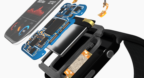
Smartphones and Foldable Devices
The internal structure of modern smartphones and foldable devices depends on rigid-flex PCBs, which create space-efficient designs. The system enables flexible display technology because it allows electrical pathways to bend while maintaining operational integrity, and it supports the compact design of complex components, which include camera systems. The design process creates smaller products that provide customers with better operational capabilities than before.
Wearable Devices
Rigid-flex PCBs build smartwatches, fitness trackers, and smart clothing products for wearable technology. The devices use their flexible design to shape their products according to body contours, which makes them suitable for use throughout extended periods. The system enables efficient sensor installation, which results in precise data monitoring.
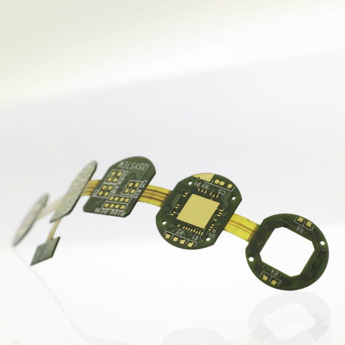
Medical Smart Devices
Rigid-flex PCBs have become the standard technology used in medical devices, which include implantable sensors, portable diagnostic devices, and health monitoring patches. The medical devices need minute, reliable parts that offer not only accuracy but also a long life cycle in critical healthcare settings.
IoT Devices
The IoT applications use rigid-flex PCBs to create efficient design solutions for smart home sensors, industrial monitoring systems, and connected wearable nodes. The system achieves compact electronic system design through space-saving capabilities, which enable operational capacity to remain intact.
Conclusion
The development of space-saving rigid-flex PCB circuits has created a new era in electronic design, which allows engineers to work beyond conventional rigid board restrictions. The PCBs create compact designs that combine rigid and flexible components into one unit that decreases space requirements while maintaining operational reliability and performance benefits.
The smart electronics revolution of today depends on rigid-flex technology, which powers smartphones, wearables, medical devices, and Internet of Things (IoT) devices. The combination of material and manufacturing technological developments with existing design and cost difficulties enables the sector to access better and more powerful technology solutions.
The space-saving rigid-flex PCB circuits will keep driving technological progress, which produces devices that use less space and require less power while providing better performance to modern consumers.
Lynn Martelli is an editor at Readability. She received her MFA in Creative Writing from Antioch University and has worked as an editor for over 10 years. Lynn has edited a wide variety of books, including fiction, non-fiction, memoirs, and more. In her free time, Lynn enjoys reading, writing, and spending time with her family and friends.